


NANBIOSIS Strengthens European Collaboration at the VI ISCIII Conference on Biomedical Research Infrastructures
NANBIOSIS joined the VI ISCIII Conference on European Research Infrastructures, strengthening collaboration with key European infrastructures and industry.
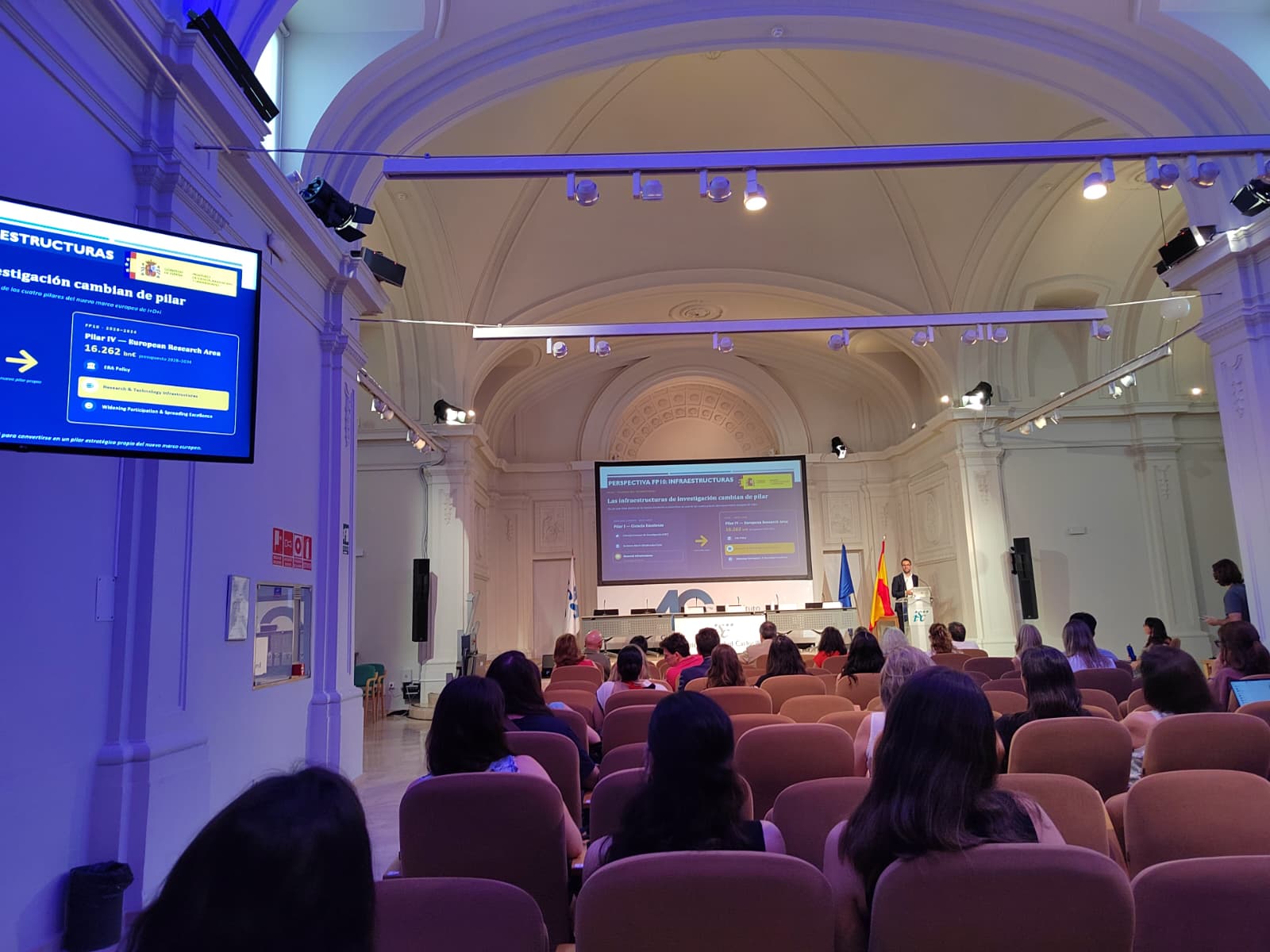
Madrid, June 2026 — Last month, on June 30, NANBIOSIS participated in the VI Conference on European Research Infrastructures in Biomedical Sciences, organized by the International Programmes Area of the Instituto de Salud Carlos III (ISCIII). The event brought together representatives of major European Research Infrastructures (RIs), research organizations, industry, and public institutions to discuss the future of collaborative biomedical research in Europe.
Held at the Ernest Lluch Auditorium on the ISCIII Chamartín Campus in Madrid, the conference highlighted the strategic role of European Research Infrastructures in advancing health research and innovation. Discussions focused on key topics including the contribution of RIs to the European Open Science Cloud (EOSC), collaboration with industry, the evolving European research landscape, and the role of research infrastructures in addressing the One Health challenge.
The programme featured experts representing several European Research Infrastructure Consortia (ERICs), including BBMRI, MIRRI, ERINHA, Euro-BioImaging, EU-OPENSCREEN, EATRIS, ECRIN, ELIXIR, INSTRUCT, and INFRAFRONTIER, offering attendees an overview of current initiatives and future opportunities for international collaboration.
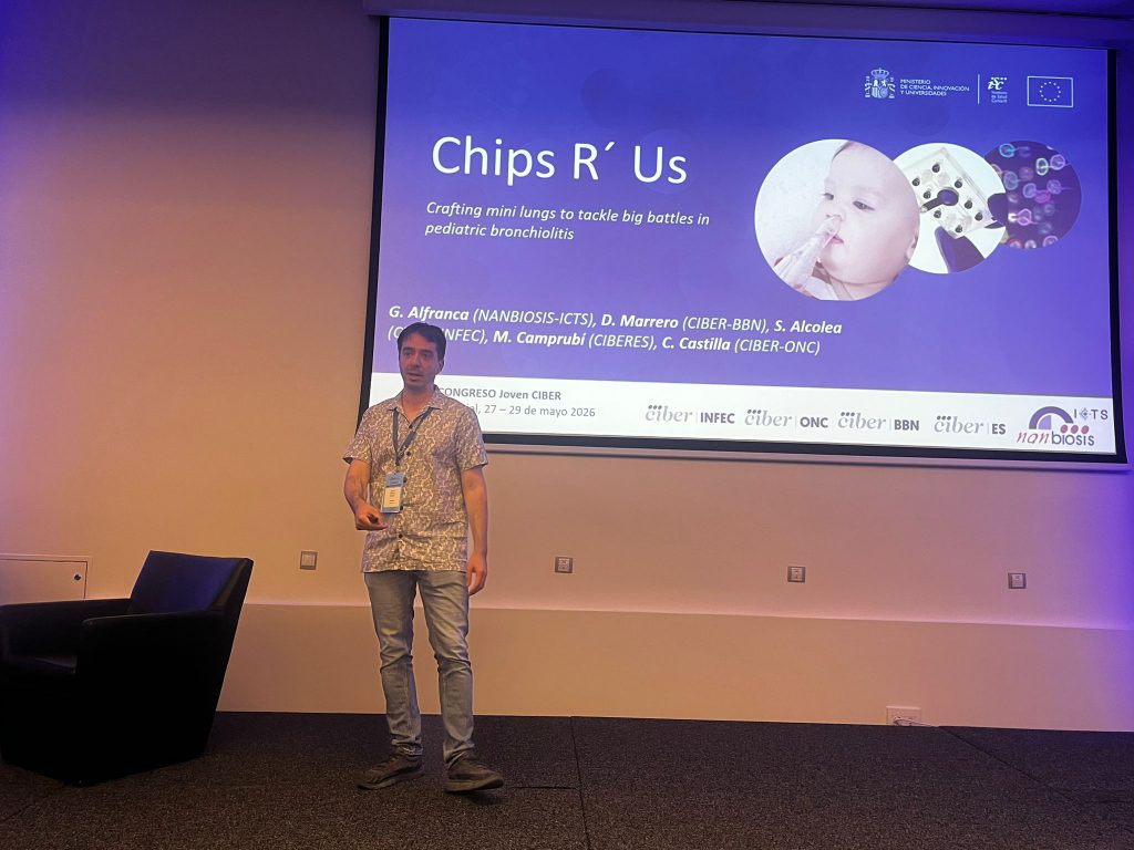
NANBIOSIS was represented by Gabriel Alfranca, Communication and Internationalization Manager, who participated in the dedicated networking session held after the conference. This space enabled direct discussions with national coordinators of European Research Infrastructures, facilitating new contacts with leading research infrastructures and companies interested in collaborative opportunities within the European biomedical innovation ecosystem.
Participation in events such as this reflects NANBIOSIS’ commitment to expanding its international network, fostering strategic partnerships, and increasing the visibility of its advanced biomedical services within the European Research Area. Strengthening connections with complementary infrastructures and industrial stakeholders supports NANBIOSIS’ mission to provide cutting-edge technologies and expertise to the scientific and innovation communities.
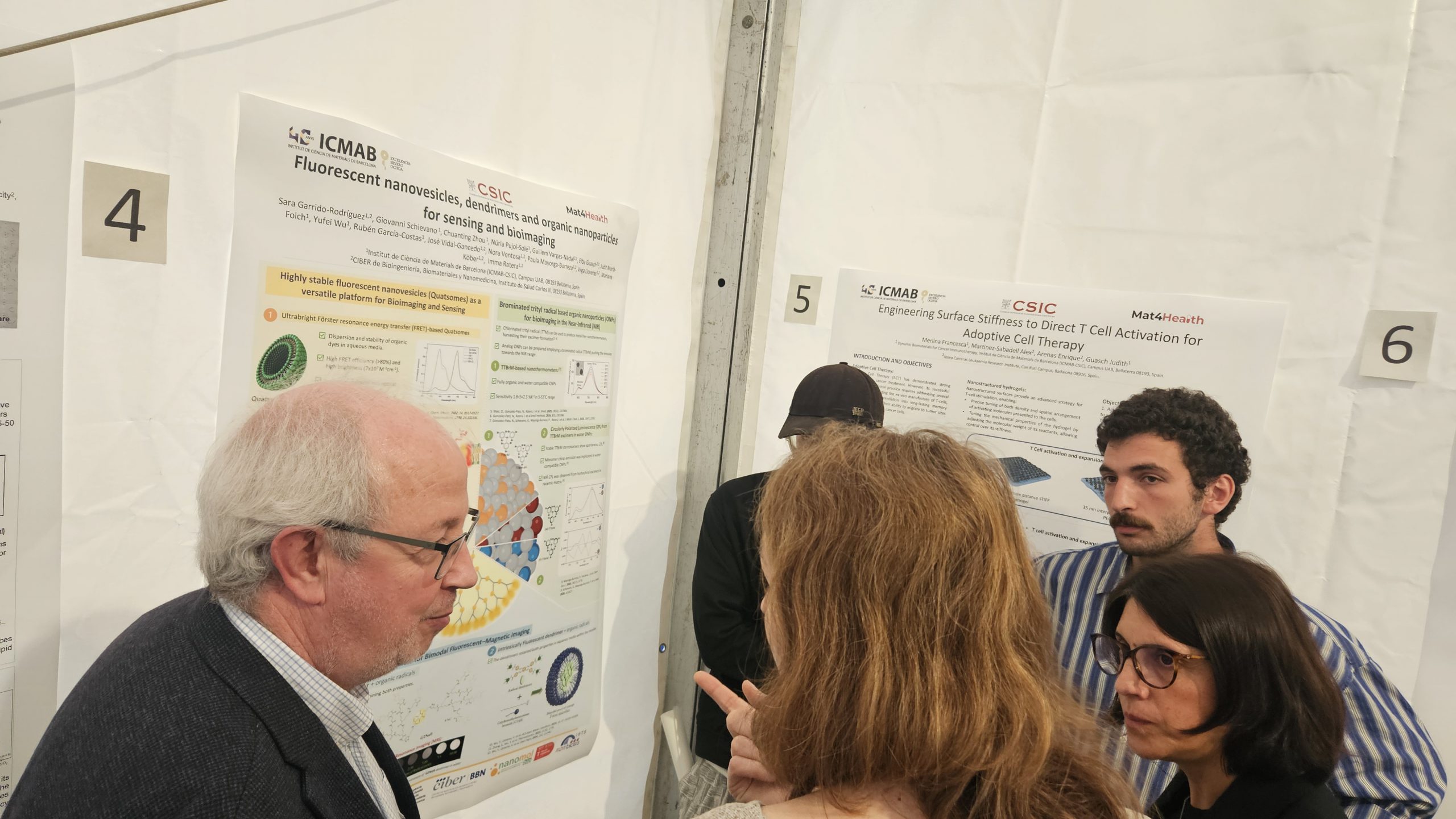
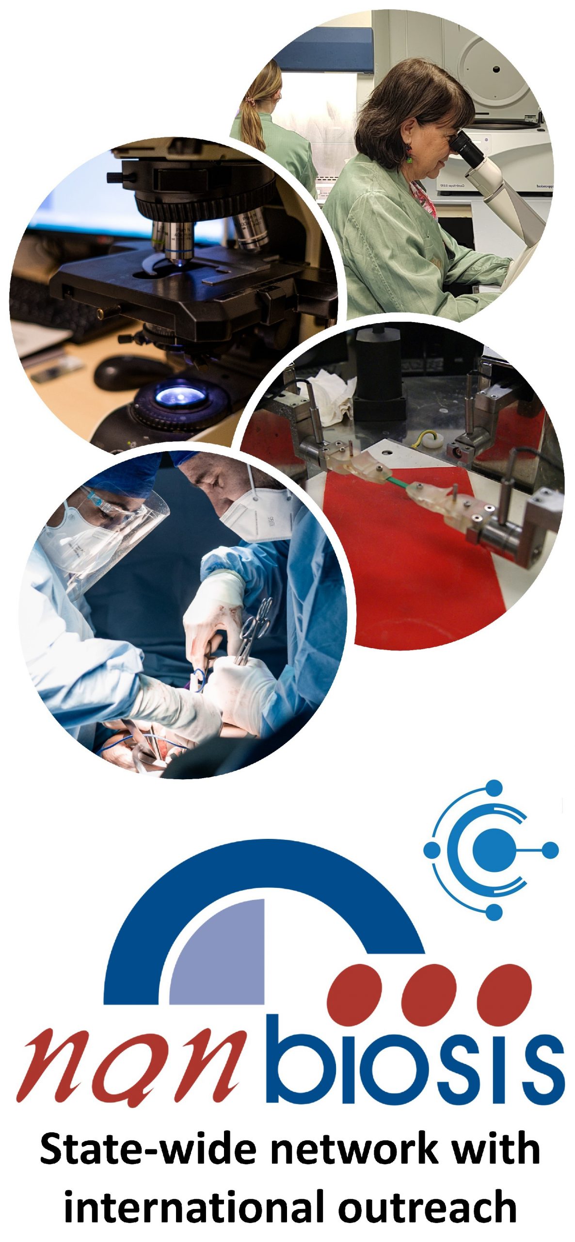
What is NANBIOSIS?
The goal of NANBIOSIS is to provide comprehensive and integrated advanced solutions for companies and research institutions in biomedical applications. All of this is done through a single-entry point, involving the design and production of biomaterials, nanomaterials, and their nanoconjugates. This includes their characterization from physical-chemical, functional, toxicological, and biological perspectives (preclinical validation).
If you want to collaborate with us, visit our Order Request page.
In order to access our Cutting-Edge Biomedical Solutions with priority access, enter our Competitive Call here.
NANBIOSIS has worked with pharmaceutical companies of all sizes in the areas of drug delivery, biomaterials and regenerative medicine. Here are a few of them: